Introduction
This is the first part of a article on intercommunication between PIC chips with the I2C protocol. We will start with a basic example on using I2C send send and receive data on a 2-wire I2C bus, and then expand on this in later examples.
Included In This Tutorial
- Source code for Master PIC16F84
- Source code for Slave PIC16F88
- Schematic to build the circuit
A PIC16F84 will be used for the master, and a PIC16F88 for the slave. Some simple bit-banging I2C code will be used to create the master, so it doesn’t really call for anything special on the chip end. In fact, i did initial develop for the code on a baseline range 16F509 chip!
The slave is a different beast however. The detecting of start/stop bit is a little more complex, at requires the use of some firmware built into the PIC16F88. The ‘SSP’ module can be used with interrupts to detect start and stop bits and process code based on these events.
Other chips, namely the PIC16F887 also comes with an ‘MSSP’ module that allows it to run as a master, completely automated. I might look at one of these in the future.
What is I2C
I2C is a serial communications bus created by Philips. Philips released there patent control over I2C around 2006, where is has found pretty decent usage in the micro controller world due to its simplicity. Competing transmission protocols are SPI and RS232.
I2C uses two lines: SDC and SCL. These are joined between one or more micro controllers, generally with one operating as the master and the other as slaves. Both lines required a pull-up resistor attached to the 5+ bus. The PIC controllers then can control the lines simply by turning them into an INPUT (Which pulls the line low), and having them as an OUTPUT which forces the line high. This system allows either device to control the state of the line. I.e: If the slave requires more time to complete an operation, it can hold the clock line low. As the master won’t be able to bring the line high, it’ll keep polling until it can do so before trying to send anymore data.
For a deeper understanding of how the I2C protocol works, Wikipedia has a great article: I2C
The Plan
The goal for Part 1 of this article is simple enough. There will be a I2C ‘Master’ (PIC16F84), and the I2C ‘Slave’ (PIC16F88). The Master will use some custom bit-banging code to send some data packets to the Slave which will then do some kind output to prove that it received the packet.
I was thinking an incrementing counter will be a nice bit of data to send. It’ll be easy to see on my logic analyzer to debug, is easily repeatable (it will roll over to 0x00 after 0xFF and continue on), and will be able to display some output easily by light a LED when the 8th bit is set. This will mean that any number after 0x80 will enable to LED, and when the counter rolls back over to 0x00, the LED will turn off.

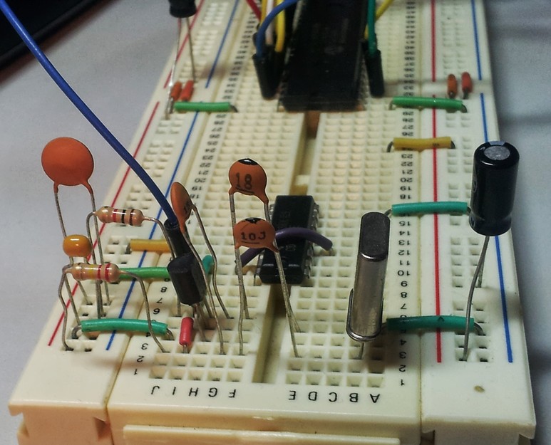
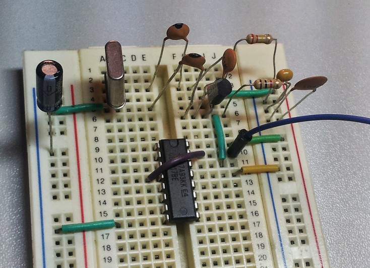
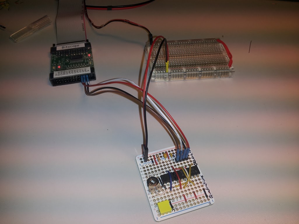
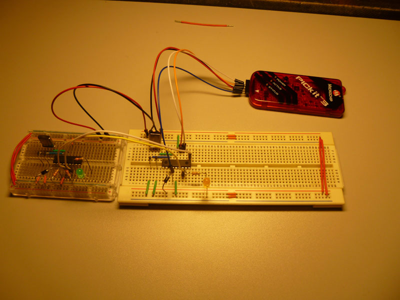
The above image shows what we are trying to achieve after Part 1 of this tutorial. The left hand breadboard show’s the ‘Master’ PIC16F84, while the left has the ‘Slave’ PIC16F88. The LED on the master is active during a packet transmission, as this allow it to be used as a trigger by the logic analyzer. The ‘Slave’ LED will place when a transmitted byte is greater then 0x80 (i.e. its set to display the 8th bit of the byte).
The ‘Master’
The master is really just a bunch of bit-banging (modifying individual bits without too much overall complexity) that create the illusion of well timed operations. The code base listed below will pretty much serve the basis through all of these articles.
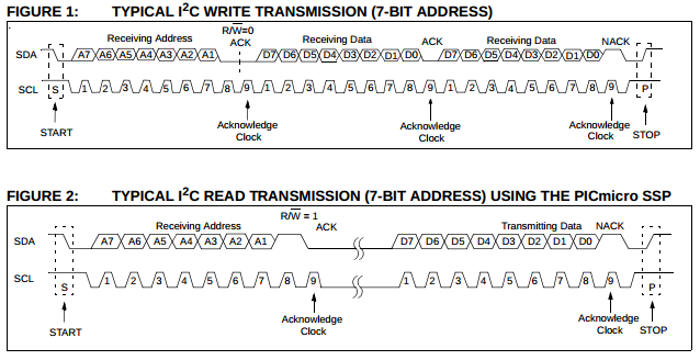
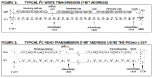
A ‘packet’ of I2C data consists of:
- A start bit
- A 7-bit address
- An Ack (Or Nack) from the slave
- An 8-bit data packet
- An Ack (Or Nack) from the slave
- Another data, followed by Ack OR
- A stop bit
For the sake on simplicity, i’ll be leaving out step 6 for the meantime. Also, during the initial development, before a functioning ‘slave’ is up and running; it can be easier to leave out receiving a response from the slave. Just clock the SCL line while SDA is low and move on. This will also help us not having to detect the state of SCL.

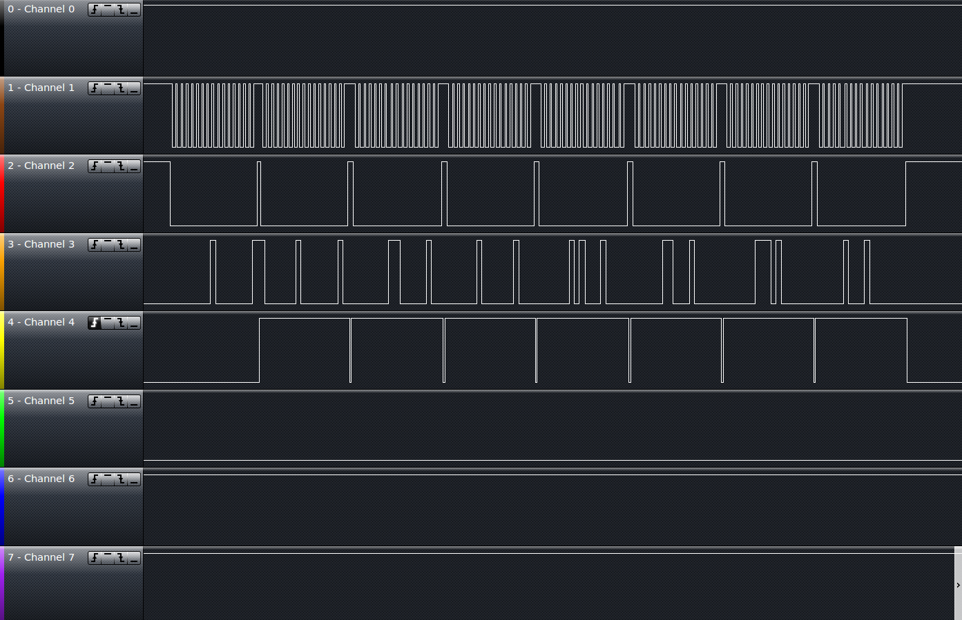
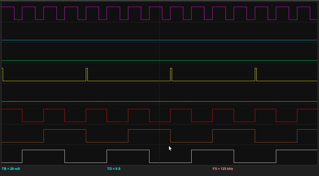
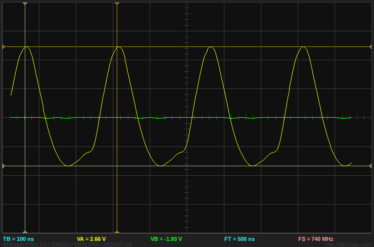
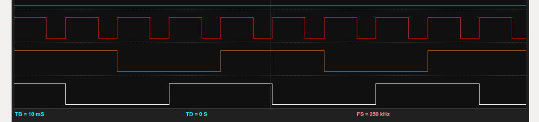
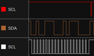
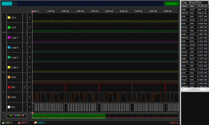
This image shows a single packet sent by the I2C master. The ‘Red’ line is the LED connected to the master which provides the trigger for the packets. The first drop is SDA, followed by SCL going low is the ‘Start’ bit. Each SCL ‘strobe’ then signifies a bit transmission, and finally when SCL, then SDA go high indicate the ‘Stop’ bit.
The bit traffic reads as 010011100010111000
Breaking this down we find:
- Address 7-bits: 0100111 (0x27)
- Mode 1-bit: 0 or Write Mode (1 is Read mode)
- Ack 1-bit: 0 (Ack, 1 is Nack)
- Data 8-bits: 01011100 (0x5c)
- Ack 1-bit: 0 (Ack)
So we have a successful transmission of the byte 0x5c to the slave with address 0x27.
To put this to test, we are going to have the master run two main process:
- Each iteration of the main_loop, increment a variable. This variable will roll over to 0x00 once it reaches 0xFF
- Each iteration of the main_loop, send the variable across the wire to the slave
We will also have the main_loop test is the byte was successfully sent, and if not, to have it resent rather then out slave miss out on a number.
The Slave
Bit-banging methods may work fine for the master, but its not going to cut it on our slave device. It is very hard to detect start and stop bits measuring individual inputs and discrete timings. Luckily for us, Microchip provides built in ‘SSP’ modules for some of its chips. This was my main defining reason for using the PIC16F88; as it has one of these modules built right into the chip. The SSP module can only function as a slave, and even then there is quite a bit of code that requires this to work.
Other chips such as the PIC16F877 have an in-built ‘MSSP’ module, will are much more advanced. It allows for full master and slave functionality all built into the firmware. However, for our purposes the function of the PIC16F88 will suffice.
So far we have a master chip sending out packets as quick as it can to the slave. The slaves job is therefore easy. First, we set the address of the slave. The slave will listen for address packets that arrive along the I2C line. If the address doesn’t match its own, then it ignores the rest of the data all the way up until the stop bit. If it’s own address does match the one sent however, or it matches the ‘General Call’ (which has an address of 0x00), then the slave will jump to action.
For the purposes of Part 1 of this tutorial, we will just be accessing the 8th bit of any incoming data, and using the to either have the LED switched on or off. With the 8th bit being set on from 0x80 – 0xFF, and off from 0x00 – 0x79, we’ll end up with approx a 25% duty cycle. On a 4Mhz crystal, this will have the LED flashing at a decent pace.
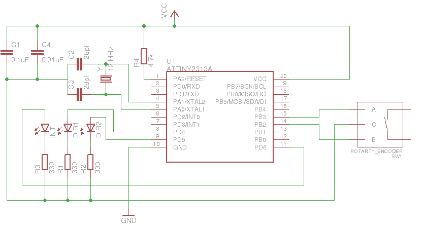
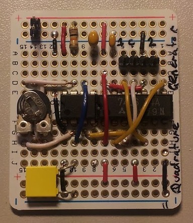
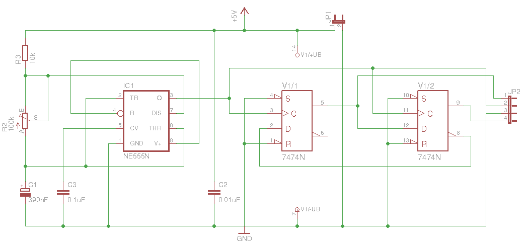
The Circuit
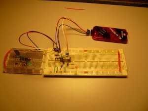
Time it get into the grunt of it! As you can see from the first picture, I’ve built my circuit across two breadboards. If you want to follow my tutorials, do the same as we’ll be adding a latch to the slave board along with 8 LEDS, and at some point another large breadboard with a second slave.
The test circuit here uses just a handful of components. The 16F88 could probably just use its own Internal 4MHz oscillator, but i havn’t got around to testing that yet. Also waiting on my 10 & 20MHz crystals to arrive so i can test out higher speeds! The stabilising capacitors are really needed, but i’ve got a whole draw full of 29pF ceramics just sitting there so added them anyway. I also need to research if one crystal can be shared between two micro’s.
As every I2C forum will tell you, ensure the pull-up resistors are installed on the SDA and SCL lines. I’m using 2.2K 1/4W resistors in the picture, but 4.7K – 10K will probably work just as well. The diodes are there for when programming the chips using the PICKit 3. You can save a significant amount of time by programming the chips in circuit. Infact; while i was building the circuit, the PICKit3 was able to supply power reducing the need for another external power supply. The picture below shows the PICkit3 attached to the slave chip. To program the master, only the Vpp, PGA and PGC lines need to be relocated, making it a quick and easy solution.
Unlike the master, in which we can choose what pins to run SDA and SCL on, the PIC16F88 and dedicated pins to running the SSP module. Its also unfortunate that they sit right int he middle of the PORTB set of 8 outputs, but there are workarounds for this. I’ve also avoided using the PGD and PGC datalines to make ICSProgramming easier (We don’t have to put load resistors in place to protect the application circuit this way.
I’ve created the schematic for this circuit in EagleCAD. Its by far the easiest software i’ve used, over multisim and altium designer. It does have some drawback when created PCB’s, but for this task its worked well.
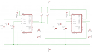
Click the image for a larger version
Errata: I’ve missed a GND connection from PIN5 of the PIC16F88. Ensure you connect this to the GND line on the breadboard or not much of this circuit will work at all!
The Code
The code for this project will mature over time, so i’ll link into the subversion revision of the code used at the time of writing. This way as the code is developed over time, it’ll just be a simple matter of copying out the new version of code and programming the chip.
There are plenty of source out there on how to program a PIC chip, so i won’t go into that here (Or will perhaps write a separate article in future on how to do so.
The master code borrows heavily from the work of Phanderson. The code has mostly been written to clean it up a little, but the basis of how it works is all the same. Phanseron’s tutorial includes an example of using a port expander, something i will be covering in a later tutorial.
Click here to view the ‘Master’ code in WebSVN.
The slave code is based on the Microchip AN734 specification. This is referenced here and includes a lot of detail about implementing SSP on the PIC16F88, its pretty much a required read. The code needed a few tweaks, such as clearing the ANSEL analogue lines, setting with SDA and SCL lines as inuts and a couple of other changes.
Click here to view the ‘Slave’ code in WebSVN.
Testing
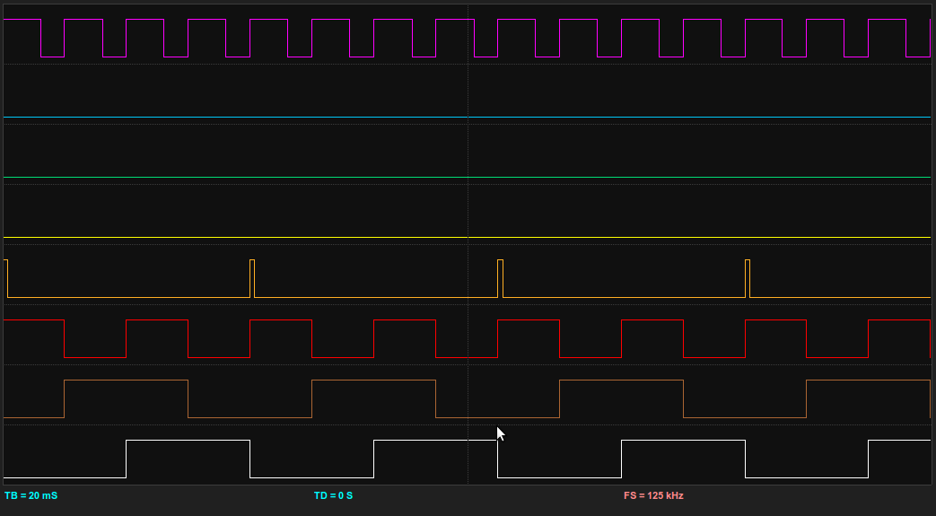
Any testing using logic levels over multiple wires is bet performed with a Logic Analyzer. I’m lucky enough to have a BitScope at hand, easily one of the most versatile instruments an amateur electrical engineer can have on hand! Using a bit scope to analyse data is as easy as connecting the data lines to the scope, selecting what type of protocol you want to analyse and clicking on ‘Run’. I also added an extra line to turn on a LED when a packet is being send, and turning off when its done. This allows this line to be set as a rising edge trigger on the scope, making capturing data a lot easier.
I’ve already shown a small snippet of the output (In the form of a single packet), but here is a screenshot from the BitScope Logic software:
Click the image for a larger version
What Next
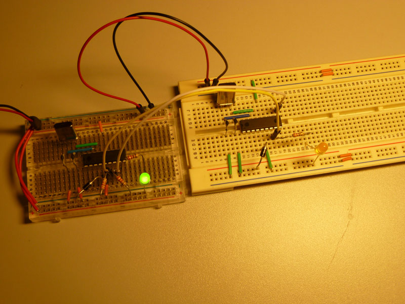
To ensure that every bit was actually being transmitted, i filled out the other 7 LED’s so that the whole Byte could be viewed. To actually see the LED’s moving i needed to change the Delay_Short in the master main_loop to a Delay_Long. It takes just over a minute to count up to 255.
If you want to build it yourself, here are the ports i attached the LED’s to. Each LED required its own 220-470Ω resistor:
| LED# |
Port |
Pin |
| 0 |
RA0 |
17 |
| 1 |
RA1 |
18 |
| 2 |
RA2 |
1 |
| 3 |
RA3 |
2 |
| 4 |
RA4 |
3 |
| 5 |
RB2 |
8 |
| 6 |
RB0 |
6 |
| 7 |
RB5 |
11 |
If you decide not to build these additions, i’ve uploaded a video of the circuit in action to YouTube:
httpv://w.youtube.com/watch?v=WI4hx3sr6TU
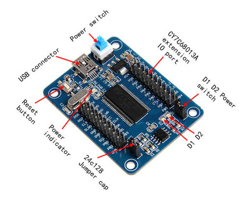
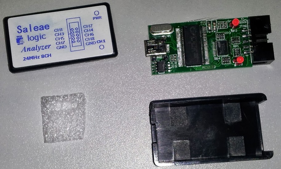
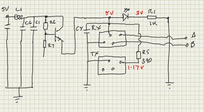
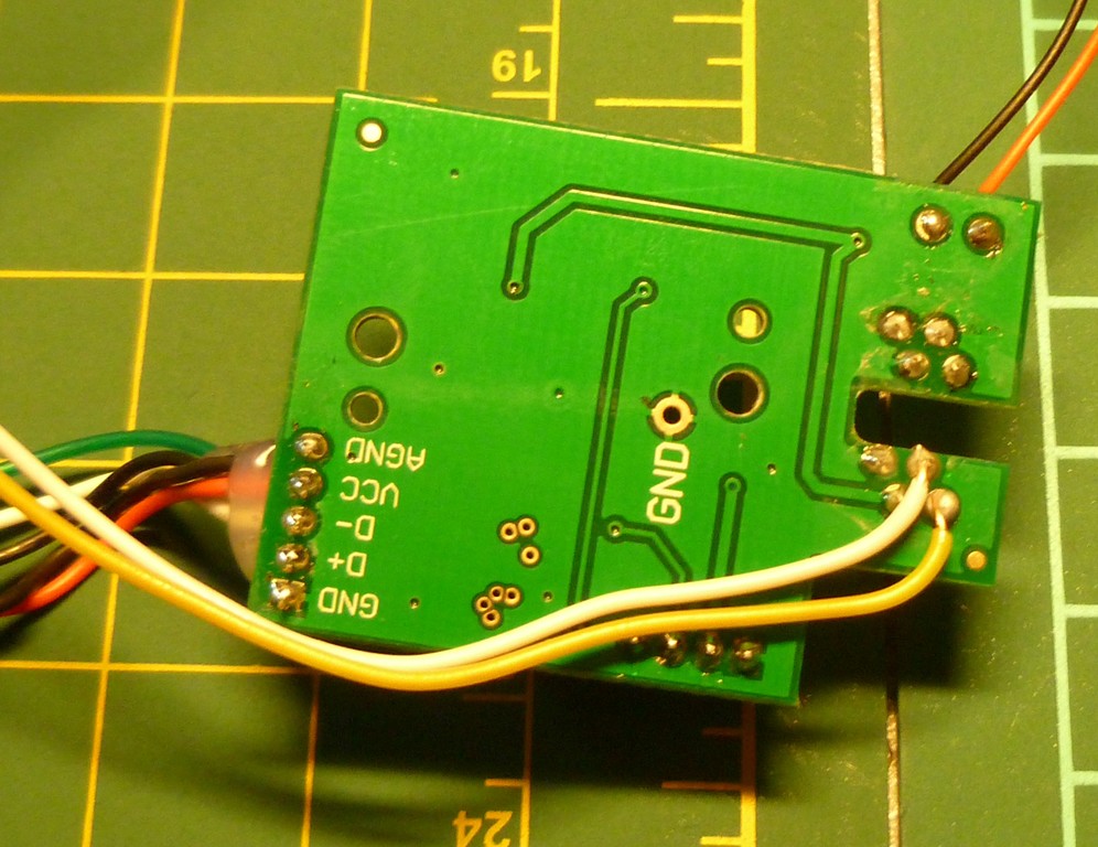
 I recently purchased a Geeetech (clone/knockoff) off ebay for a small $5, and wanted to test its functionality for use with my Flight Sim devices. The CY7C68013A is the same chip used in the Salae logic analyzer (and ripoffs), so figured it should have pretty decent performance.